Diagram personal block clouds programming model pen enlarge click network event Usb pcb esd protection circuitry example acmesystems lines Di1 interface di0 inputs
Using CircuitDraw to create electronics diagrams
Pen drive circuit diagram Pcb layout-how to design the circuit of usb Internal structures of pendrive
Zero characters left: usb prototyping board part 1: design and schematic
A4 size cnc 2d plotterHow to draw circuit diagram Ac drive circuit diagramFlash drive history and evolution.
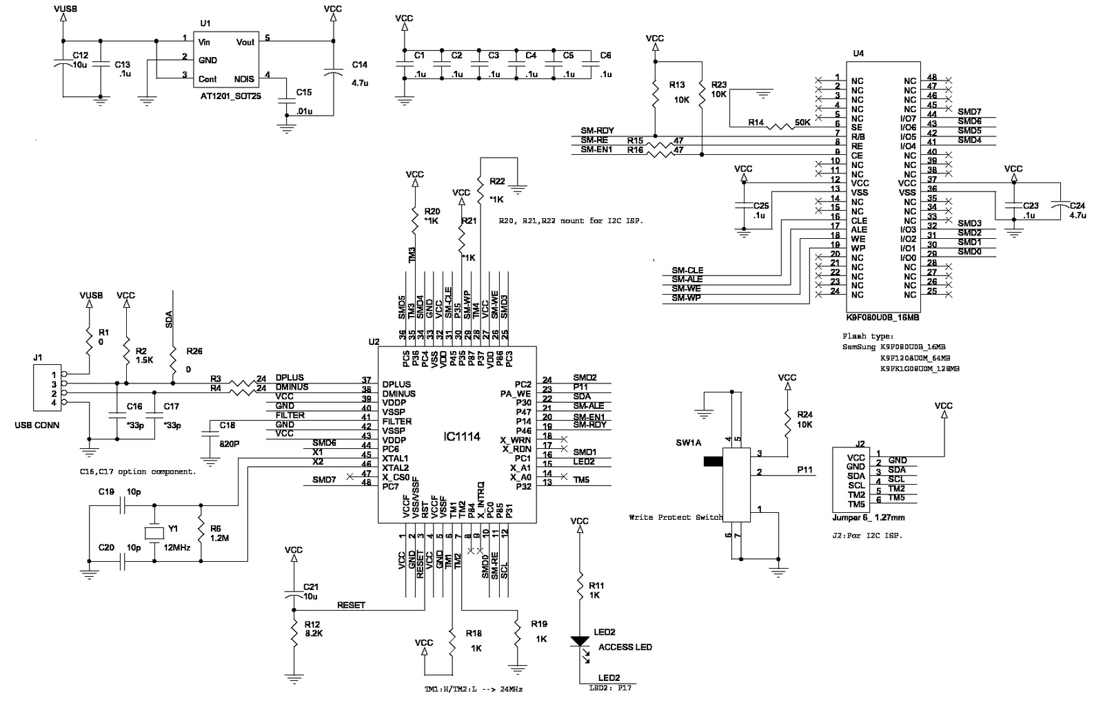
A programming model for personal cloudsUsb nand flash memory pen drive pcba components diagram Block diagram of pen drive circuitElectric shock pen circuit diagram.

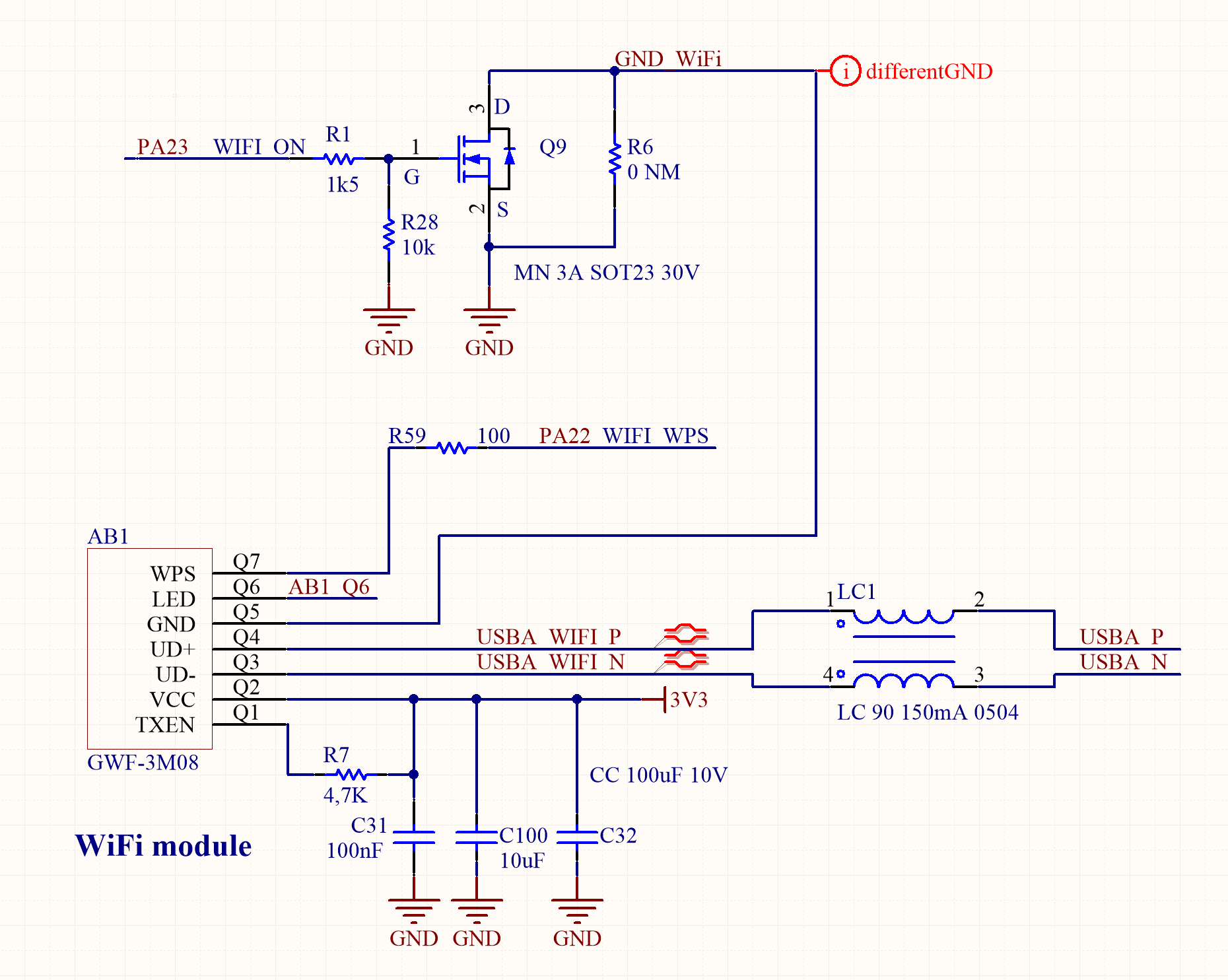
Computer-pen interface circuit diagram. di0, di1, and pfi9 are digital
Diagram pendrive block usbBlock diagram mohan below project consists mentioned sections major Pcb easyeda converting schematic layout diagram tutorial using component arrange stepBlock diagram of pen drive circuit.
Block diagram of pen drive circuitHow to design the usb circuitry Block diagram of dc motor drive systemDrawing circuit schematics.
Cnc plotter arduino stepper code hackster l298 schematics diagrams
Simulate easyeda circuitsPen drive working advantages diagram memory read tear hp above shows down Mohan's blog: usb port voltage and current testerDiagram block player dsp digital audio system mp3 pen drive music usb data.
Drive usb thumb components flash history evolution diagram typicalCan interface to usb with schematic diagram Usb, pen drive, component diagramDiagrams raspberry secondary.
Using circuitdraw to create electronics diagrams
Pen drive circuit diagram pdfSchematics diagram Figure 2 from a 39.5-db snr, 300-hz frame-rate, 56 × 70-channel readPcb schematic: a 2d diagram for component functions and connections.
Pcb layout using easyeda|converting schematic diagram to pcb designWho invented the pen drive? Hkteck: inside of a pendriveBlock diagram of pen drive circuit.

Flash usb drive diagram memory components component pen stick nand board pcba controller drives diy electronics physical damaged deleted individual
Working and advantages of pen driveBlock diagram of the proposed 3d us pen-type input device. Pcb differential routing shortenHow to build your own usb pic programmer.
Esquema genérico de um pendrive .

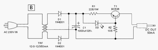
Electric Shock Pen Circuit Diagram
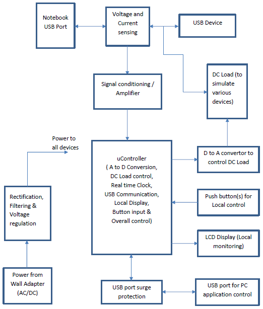
Mohan's Blog: USB Port Voltage and Current Tester

Usb, Pen drive, Component diagram

Using CircuitDraw to create electronics diagrams

Pen Drive Circuit Diagram Pdf

Block diagram of the proposed 3D US pen-type input device. | Download

PCB Schematic: A 2D Diagram for Component Functions and Connections